Invited Speakers
S1. Nanophotonic Materials and Devices
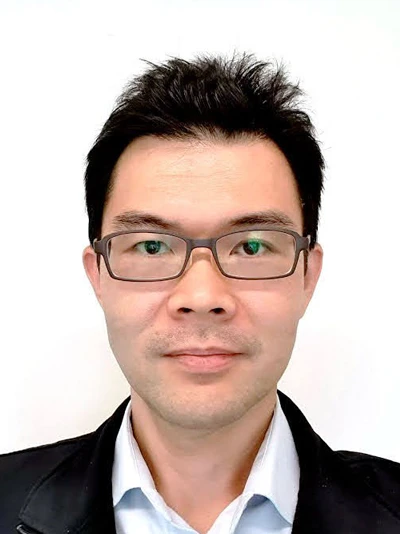
Joel Yang
Professor, Engineering Product Development, Singapore University of Technology and Design, Singapore3D Printing With Light For Light
3D printing is a cost-effective and convenient means to produce prototypes and test out designs. In our lab, we use high-resolution 3D printers based on two-photon polymerization lithography (TPL) with 780 nm wavelength femtosecond lasers to quickly realize nanoscale structures that are in turn designed to control light. The use of TPL, an additive manufacturing process with sub-micron print resolutions, to produce structures for optical effect is a relatively new endeavor [1].
We demonstrated the printing of structural colors, generated from nanoscale features of dielectric materials. We have previously shown the fabrication of nanopillars, gratings, mesh-like, and wood-pile photonic crystal structures that appear colorful under white-light illumination. The ability to achieve a wide range of colors by simply tuning geometric properties opens fascinating opportunities to the nanoengineer or nanoscientist to design colors using material properties, and nanostructure geometry as input parameters. This physical approach differs from the chemical approach for synthesizing pigments and dyes, where colors arise due to optical absorption.
We now demonstrate the integration of these structural colors with other micro-optical elements, such as microlenses and spiral phase plates. Equipped with TPL as a nanoscale 3D printer, structural color geometries are conveniently integrated in a single print run with other user-defined optics. Doing so enables one to produce structured light from incoherent light sources, holographic color prints, and control of the light-field for 3D representation. We will discuss the use of structural colors combined with micro-optics for enhanced information content and optical security [2].
- References
- Hao Wang, et al. “Two-Photon Polymerization Lithography for Optics and Photonics: Fundamentals, Materials, Technologies, and Applications”, Adv. Funct. Mater. 2214211 (2023)
- Hongtao Wang, et al. “Coloured vortex beams with incoherent white light illumination”, Nature Nanotechnology 18, 264-272 (2023)
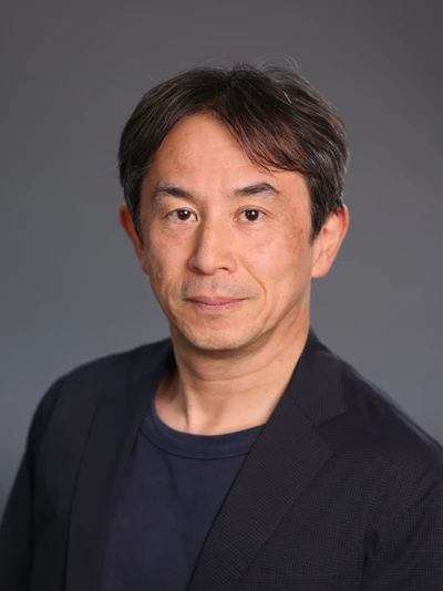
田中拓男 Takuo Tanaka
Professor, Institute of Physical and Chemical Research (RIKEN), JapanMetasurfaces for sensing applications
Takuo Tanaka is a chief scientist of RIKEN. He received his PhD degree in 1996 from Osaka University. After that, he joined faculty of Engineering Science, Osaka University as an assistant professor. In 2003, he moved to RIKEN as a research scientist in Nanophotonics Laboratory. He was promoted to associate chief scientist in 2008 and to chief scientist in 2017. Now he is heading another research lab. “Innovative photon manipulation research team” in RIKEN as a team leader. In addition, he was appointed as a visiting professor in Saitama university from 2010, as an adjunct professor in Gakushuin university from 2012, as a visiting professor in national Tsing Hua university from 2017, as a specially appointed professor in Tokushima university from 2019, and as a visiting professor in the university of the Philippines Diliman from 2019.
His research background is three-dimensional microscopy such as confocal microscopy and two-photon microscopy. Recently, his research fields are gradually shifted to nanophotonics, plasmonics, and metamaterials with developing many new nanofabrication techniques. He has also experimental and theoretical experiences about high precision optical measurements and spectroscopy, and numerical computation of the interaction of light with structured materials. Tanaka is elected as a fellow of JSAP.
Highly sensitive sensing techniques for biological and chemical materials are becoming increasingly essential in our daily lives. Recently, metasurfaces have been employed to enhance the sensitivity of infrared (IR) spectroscopy.
We have applied a metasurface absorber, consisting of a metal-insulator-metal (MIM) structure, to background-suppressed IR spectroscopy for detecting organic molecules. Due to plasmonic enhancement and resonant coupling between excited plasmons and molecules, molecular sensitivity at the atto-molar level has been achieved.
For liquid samples, we proposed a 3D metamaterial device incorporating nanofluidics to precisely guide target molecules into the hot spot region of the metasurface, resulting in ultra-high sensitivity for IR absorption detection. The device structure comprises a metal square-disk array and a metal mirror, separated by a nanofluidic channel. Using this device, sensitivity at a molecular density of approximately 10-4 molecules/Å2 was achieved.
The sensitivity also depends on the density of hot spots within the metasurface. To increase the density of these hot spots, we designed and fabricated a vertically aligned MIM (v-MIM) structure with a nano-gap of 25 nm. This metasurface device was applied to the detection of carbon dioxide and butane, with designed resonances at 4033 cm-1 and 2945 cm-1, corresponding to the C=O and -CH2 vibrational modes, respectively. Due to its compact size, the v-MIM structure enables increased integration density, allowing the detection of a 20 ppm concentration with suppressed background noise and high selectivity in the mid-infrared region.
Additionally, we introduce a metasurface-based immunochromatography device for biomolecular sensing.
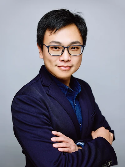
黃耀緯 Yao-Wei Huang
Assistant Professor, Department of Photonics, National Yang Ming Chiao Tung UniversityMetasurface-based depth sensing and topology optimized high-Q metasurfaces
Dr. Yao-Wei Huang is an Assistant Professor of Photonics and Yushan Young Scholar at National Yang Ming Chiao Tung University (NYCU). He is also a Fellow of the Higher Education Academy (HEA). Dr. Huang has extensive research experience from prestigious institutions such as Harvard, Caltech, and NUS. His expertise spans nanophotonics, physics, materials science, nanofabrication, and nanotechnology, and he earned his Ph.D. in Applied Physics from National Taiwan University.
Dr. Huang's research focuses on nanophotonics, metasurfaces, inverse design, nonlocal effects, structured light, dispersion engineering, and computational visual sensing, with innovative applications in extended reality and LiDAR. He has authored and co-authored over 60 scientific publications, proceedings, and patents, including articles in Nature Photonics, Nature Communications, Proceedings of the IEEE, Science Advances, Nano Letters, etc. His contributions to the field have been recognized with awards such as the Google Gift, and his research aims to advance metasurface technologies for the betterment of human well-being.
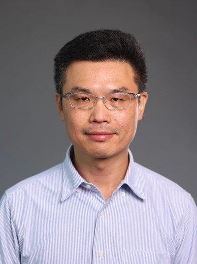
陳國平 Kuo-Ping Chen
Professor, Institute of Photonics Technologies, National Tsing Hua UniversityEnhancing Light-Matter Interactions in 2D Materials with Nanophotonics
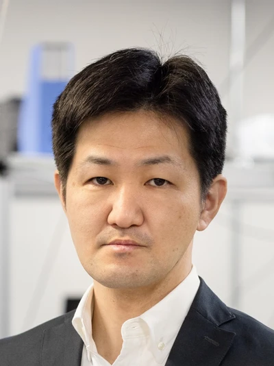
小西邦昭 Kuniaki Konishi
Associate Professor, Institute for Photon Science and Technology, Graduate School of Science, University of Tokyo, JapanLightwave control using free-standing dielectric nanomembrane structures
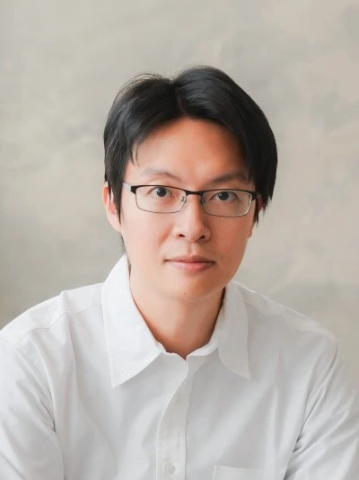
何亜倫 Ya-Lun Ho
Senior Researcher, Research Center for Electronic and Optical Materials, National Institute for Materials Science, JapanMembrane Nanophotonic Platform for Enhancing Light-Matter Coupling in 2D Transition Metal Dichalcogenides
Ya-Lun Ho received his B.S. and M.S. degrees from National Taiwan University in 2009 and 2010, respectively, and his Ph.D. from The University of Tokyo in 2015. From 2014 to 2017, he was a JSPS Research Fellow, followed by his role as an Assistant Professor at The University of Tokyo from 2017 to 2022. Since July 2023, he has been a Senior Researcher at the Research Center for Electronic and Optical Materials, National Institute for Materials Science (NIMS).
Ya-Lun Ho's research focuses on nanophotonics and plasmonics based on 2D and low-dimensional materials, with a current emphasis on atomic-layer and membrane metasurfaces. His expertise lies in the design and fabrication of advanced nanophotonic platforms, optimized for a diverse array of photonic and optoelectronic applications.
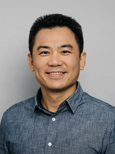
黃哲勳 Jer-Shing Huang
Professor, Research Department of Nanooptics, Leibniz Institute of Photonic Technology, GermanySubstrate Effect on the Whispering-Gallery Modes in π-Conjugated Polymer Microspheres
S2. Optical Waveguides and Communications

Christina Lim
Professor, Department of Electrical and Electronic Engineering,, The University of Melbourne, AustraliaOptical Wireless Convergence: Next-Generation Optical Crosshaul Networking

宋峻宇 Jiun-Yu Sung
Professor, Department of Electronics and Computer Engineering, National Taiwan University of Science and TechnologyOverviews of Indoor Infrared Optical Wireless Communications (IR-OWC)

Chun-Wei Chen
Postdoctoral Scholar, Edward L. Ginzton Laboratory, Stanford University, USATaming the beasts: wavefront shaping to conquer nonlinear effects in multimode fiber amplifiers
S3. Quantum Photonics and Laser Technology
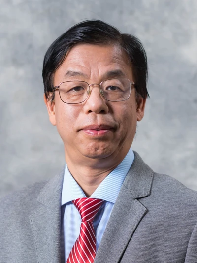
區澤宇 OU Zheyu Jeff
Professor, Department of Physics, City University of Hong KongInterferometry in the quantum age
葉文昌 Wenchang Yeh
Professor, Shimane University, JapanGrowth of crystal orientation controlled single crystal stripes in Si/Ge thin film on SiO2 for Si photonics
He is a Professor in the Department of Applied Physics, University of Shimane, Japan. He was a professor in the department of electronics, National Taiwan University of Science and Technology, Taiwan, from 2002 to 2009. He received his Ph.D. degree in engineering from Tokyo Institute of Technology, Japan, in 2000. His current research interests are formation of single crystal semiconductor thin film on SiO2 and its application to 3D-LSIs.
Formation of single crystal film on SiO2 is a bottleneck technology for future 3D-LSI or Si photonics. I will introduce our original technique for formation of semi-infinite long (001) textured Si single crystal stripes with width of ~8µm in a 60nm-thick Si/Ge films. The stripes can be thickened to 0.5 µm for formation of NIR waveguide. Transmission loss of NIR light can be much lower than that of poly-Si films since there is no energy states originated from grain boundaries. MOSFETs fabricated on the 60nm-tick stripes shows characteristics and deviations comparable to that of FD-SOI-MOSFETs.
陳俞辰 Yu-Chen Chen
Assistant Research Fellow, Research Center for Applied Sciences, Academia SinicaEngineering and characterizing single spin defects in wide bandgap materials
In these two decays, not just scientists devote to quantum technologies research, but also many countries have successively executed national quantum technologies programmes. Among all quantum technologies candidate systems, optically active spin defects in wide bandgap materials, such as diamond and silicon carbide (SiC), show as promising candidates for many quantum applications at room temperature. [1,2]. In order to achieve scalable devices, spatially precise generation of high-quality single colour centres on demand are essential. In this regard, ion implantation method has been used to engineer colour centres with high spatial accuracy [3,4], but comes at the expense of creating considerable residual lattice damage, which degrades their spin and optical coherence properties.
This talk will first give introduction of the single spin defect properties for quantum applications to provide broad idea of the quantum applications. In order to achieve scalable devices, spatially precise generation of high-quality single colour centres on demand is essential. We developed a method to use single, femtosecond pulses laser (λ = 790 nm, t = 250 fs) to generate an array of NV- centres in a CVD diamond. The positing accuracy of the generated NV- centres were determined to be about 200 nm in x-y plane. The T2 spin coherence times were measured up to 700 µs. Some NVs showed narrow, stable zero-phonon-line (ZPL), including a selection which are at the lifetime-limited linewidth of 13 MHz at 4 K. These indicate the laser writing method can generate the NV- centres with almost perfect spin and optical coherence properties.
I have also characterized unknown single spin defects in hexagonal boron nitride 2D materials. we have found a set of isolated optical emitters embedded in hexagonal boron nitride that exhibit optically detected magnetic resonance. We also demonstrated that one of them is single spin defect. The defect spins show an isotropic ge-factor of ~2 and zero-field splitting below 10MHz. The photokinetics of one type of the defects is compatible with ground-state electron-spin paramagnetism. We extracted spin-lattice relaxation times T1 of 13-17 μs with estimated spin coherence times T2* of around 40-60 ns. We also investigated into the spin dynamics and provided a simple model of the electronic structure.
Saulius Juodkazis
Professor, Swinburne's Optical Sciences Centre, Swinburne University of Technology, AustraliaHigh Intensity Laser Patterning: Nanoscale Resolution over Large Areas
Saulius Juodkazis is Professor and Deputy Director of the Optical Sciences Centre at Swinburne University of Technology, Melbourne, Australia. In 1998, he received his PhD (cotutelle) in experimental physics and material sciences jointly from Vilnius University, Lithuania, and Lyon-I University, France.
His current interests are in the fields of light-matter interactions occurring in small space (nanoscale) and time (femtoseconds) domains. He planned, established, and directs a multi-user Nanotechnology facility at Swinburne open to the Australian National Fabrication Facility ANFF users from December 2011. His research is focused on applying principles of light-field enhancement and its spectral control for applications in micro-optics, solid-state lighting, and solar energy conversion.
Professor Juodkazis has contributed to the development of a three-dimensional laser printing with nano-/micro-scale precision using femtosecond laser for applications in opto-fluidic, micro-optics, optical memory, and photonic crystals. He has shown experimentally the creation of high-pressure density phases of materials using tightly focused ultra-short laser pulses. He demonstrated that nano-textured surface of Si (black-Si) has bactericidal/biocidal property and acts as “mechanical antibiotic”, which can be mass produced. This work received 2017 Eureka prize for scientific research in Australia. He is Fellow of the Optical Society of America (OSA) and the International Society for Optics and Photonics (SPIE).
Laser inscription of structural defects in sub-surface of dielectrics and semiconductors is made with the sub-10 nm resolution and precision by direct write. Tightly-focused ultra-short ∼ 200 fs pulses create high-intensity ≥ 20 TW/cm2 when electron tunneling becomes an important contributor to ionisation. Post-exposure annealing at ∼ 800 − 1000°C temperatures partly restores the host material with fewer defects, which are well localised and can be used as optical emitters. Also, a large area patterning of Si solar cells for efficient light trapping is presented. Above the Lambertian (ray-optics) limit of light trapping can be achieved and is transferable to the solar panel ∼ 1 m2 dimensions.
S4. Information Photonics
Zhiwen Liu
Professor, School of Electrical Engineering and Computer Science, Penn State University, USAOptical processing with reconfigurable liquid crystal based scattering media
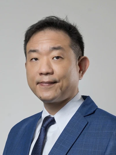
栗永徽 Yung-Hui Li
Senior Director, AI Research Center, Hon Hai Research Institute (HHRI)From Generative AI to Scientific Discovery: Foxconn's AI Innovation Journey and Future Vision
In recent years, generative AI has revolutionized various industries and research fields, marking a significant milestone in technological advancement. This keynote presentation explores Foxconn's comprehensive journey in AI development and innovation, with a particular focus on our groundbreaking achievements in generative AI applications.
The presentation begins with an overview of generative AI's fundamental concepts and its transformative impact across different sectors. We then showcase Foxconn's significant contributions to the field through our innovative solutions, including QCNet and BehaviorGPT, which demonstrate our capabilities in developing cutting-edge AI technologies for industrial applications.
Furthermore, we will unveil our strategic vision for 2025, highlighting our ambitious expansion into AI for Science. This new frontier represents a paradigm shift in scientific research, where we aim to leverage the power of generative AI to accelerate scientific discoveries, particularly in materials science.
Our vision encompasses the transformation of traditional research methodologies through the integration of advanced AI capabilities, potentially revolutionizing how we approach scientific discovery in the 21st century.
Keywords: Generative AI, Industrial AI Applications, AI for Science
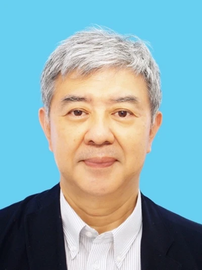
谷田純 Jun Tanida
Professor, Emeritus, University of Osaka, JapanComputational Methods for Scatter Imaging
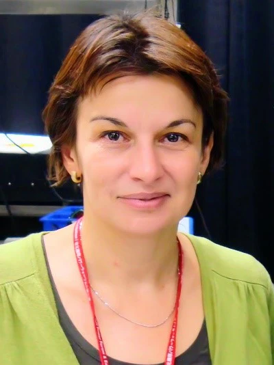
Vera Marinova
Professor, Bulgarian Academy of Sciences, BulgariaIntegration of functional nanomaterials toward opto-electronic and photonic devices
Here, we report the controlled synthesis and characterization of nanolayers (in form of two-dimensional (2D) materials and transparent conductive oxides (TCO)) and their intergation in optoelectronic and photonic devices. 2D materials have attracted intense potential for miniaturized (atomically thin) optoelectronic devices due to their layer number-dependent properties (strong intralayer covalent bonding and weak interlayer van der Waals interactions). In addition, they demonstrate extremely high optical anisotropy which gains an enormous interest for integration in ultrathin optics that allow light control at the subwavelength scale.
Another type of materials of interest are TCO layers, that prove superior performance indicating a growing demand for the next generation indium tin oxide (ITO)-free technology, including advanced display devices and dynamic flat-panel functionalities. For example, they can play multifunctional role in Liquid Crystal Spatial Light Modulators (SLM ) configurations as transparent conductive layer and as alignment layer allowing vertical alignment in LC molecules. Besides excellent phase modulation repeatability over the large-scale area, TCO's exhibits great potential for future integrated photonic devices including flexible strctures and bio-oriented technologies.
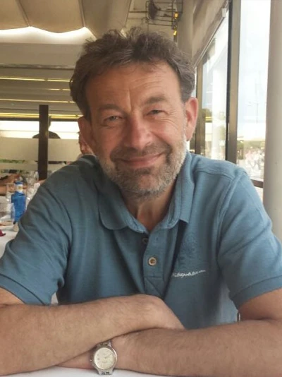
Kestutis Staliunas
Professor, BarcelonaTech, Universitat Politècnica de Catalunya (UPC), SpainPhotonic Crystal Spatial Filters
S5. Optical Design and Engineering
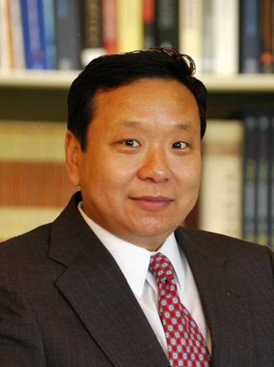
Shizhuo Yin
Professor, Department of EECS, Penn State University, USAMultifunctional crystalline materials and applications
Dr. Stuart (Shizhuo) Yin is a tenured full professor of electrical engineering at The Pennsylvania State University. He is also the Co-founder and CTO of General Opto Solutions, LLC. He is a US citizen. He received his bachelor and master degrees in Physics from Nankai University, in 1984, and 1987, respectively. He received his Ph.D. degree in electrical engineering from The Pennsylvania State University in 1993. He is an internationally known scientist in the field of advanced optical/photonic materials, devices, and their applications for optical sensing, communications, imaging, lighting, high power/energy lasers, and energy harvesting.
-
Highlights of major accomplishments
- Authored and co-authored over 300 papers in a variety of prestigious refereed journals and conference proceedings, including Nature.
- Co-authored three books in optics field: (1) Photorefractive Optics (Academic Press, 2000), (2) Introduction to Information Optics (Academic Press, 2001), and (3) Fiber optic Sensors (CRC Press, 2018).
- Awarded over twenty research projects, including the prestigious multi-disciplinary research initiative (MRI) award, funded from a variety of government agencies, industries, and private foundations with a total funding over $20 millions.
- Elected as a fellow of the International Society for Optical Engineering (SPIE) in 2004.
- Elected as a fellow of Optical Society of America in 2007.
- Won 1996 US Army Young Investigator Award.
- Won 2004 Penn State Engineering Society's Outstanding Research Award
- Won 2010 Penn State Engineering Society's Premier Research Award
- Executive committee of SPIE on Photonic Engineering
- Co-chair of SPIE on Photonic Crystal and Fiber Materials and Devices
- Expert panel for a number of government agencies, including National Science Foundation, US Army, Department of Energy, et al.
In this talk, we report our recent works related to multifunctional crystalline materials and applications. First, we address the rare earth [ytterbium (Yb)] doped lithium niobate (LiNbO3) crystalline fiber. This unique crystalline fiber has multifunctional capability, including (1) a very effective low quantum defect lasing medium; (2) an electro-optically tunable medium, in which the refractive index of medium can be quickly tuned by the applied electric field; and (3) a light guiding medium, which offers the advantages of low driving voltage and power. The Yb:LiNbO3 can be very useful for a variety of applications, including highly electrically tunable, high efficiency, highly compact lasers and tunable spectral filters. Second, we discussed micro/nanostructured functional crystalline materials, in particular, micro/nanostructured Ti:sapphire crystals. This multi-functional crystal is not only an effective wide spectral tuning range lasing medium but also an effective wavelength selective medium due to the existence of micro/nanostructures, which is beneficial for applications such as highly compact, wavelength selective lasers and filters.
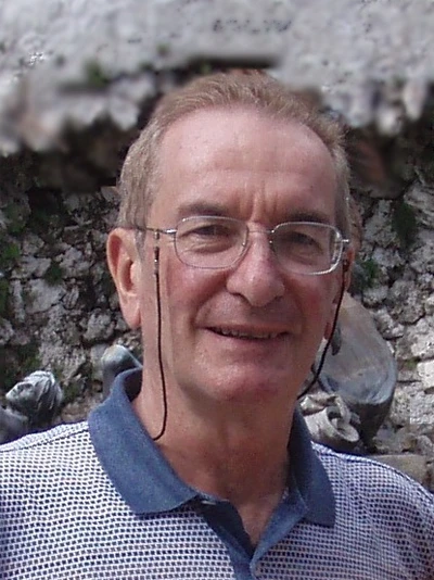
Silvano Donati
Professor, Department of Electronics, University of Pavia, ItalyNon-contact Vibration Measurements by Self-Mixing Interferometry
Silvano Donati earned a doctorate in Physics cum laude from University of Milan, Italy, and has been Full Professor of University of Pavia since 1980 before becoming Emeritus in 2015. He has authored or co-authored 350+ papers and holds a dozen patents, and has written two books, ‘Photodetectors’ (1st ed.: Prentice Hall, 2000, 2nd ed.: IEEE_Wiley 2021) and ‘Electro-Optical Instrumentation’ (1st ed.: Prentice Hall 2004, 2nd ed.: CRC 2023), covering the subject of his courses at University of Pavia and abroad. His main achievements have been self-mixing interferometry and chaos-shift-keying cryptography, the topics covered in his Distinguished Lecture talk given in 21 LEOS (now IPS) Chapters in two terms (2007-09) and continued as a Traveling Lecturer of OSA and SPIE on Self-Mixing and Lidars to date, for a total 105 Chapters visited. He has received several awards from the AEIT and IEEE, in particular the Marconi medal, the Aaron Kressel Award and the Distinguished Service Award of the IEEE Photonics Society. He was the founder (1996) and first Chairman (1997-01) of the Italian LEOS Chapter, LEOS VP Region 8 Membership (2002-04) and BoG (2004-06), and the Chairman of the IEEE Italy Section (2008-09). He has spent semesters as Visiting Professor in several Universities of Taiwan: NTU in Taipei, 2005, Sun Yat Sen in Kaohsiung (2007, 2008, 2010), NCKU in Tainan, 2012, NCHU in Taichung, 2013-14, NTUT in Taipei 2015-16 NTU in Taipei 2018-19 and NTUST in Taipei 2023. Prof. Donati is Life Fellow of the IEEE, Optica Emeritus Fellow and SPIE Life Member.
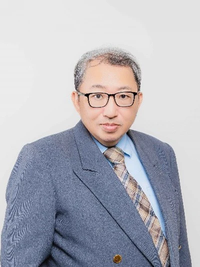
孫文信 Wen-Shing Sun
Associate Professor, Department of Optics and Photonics, National Central UniversityFull of view 50-degree projection lens design for AR glasses waveguide system
Education: PhD (1994/9 to 2002/1), Institute of Optical Sciences, National Central University.
Experience: Deputy Engineer (1990/7 to 1992/6), Institute of Opto-electronics, Industrial Technology Research Institute; Senior Engineer (1998/11 to 2002/1), Electromechanical Division, Delta Electronics Co., Ltd.; Optical consultant (2004/2 to 2005/7), Technology R&D Department, Hon Hai Precision Industry Co., Ltd.; Assistant Professor (2006/2 to 2012/7) and Associate Professor (2012/8 to present), Department of Optics and Photonics, National Central University.
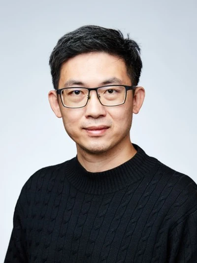
李宗憲 Tsung-Xian Lee
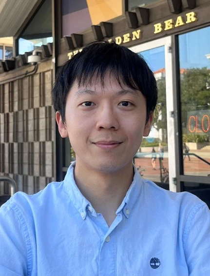
Professor, Graduate Institute of Color and Illumination Technology, National Taiwan University of Science and TechnologyLaser White Light: The Next Breakthrough in Solid-State Lighting Technology
樊俊遠 Chun-Yuan Fan
Assistant Professor, Graduate Insitute of Electro-Optical Engineering, National Taiwan University of Science and TechnologyFrom the Wave Optics to the Ray Tracing: A Novel Photonic Integrated Circuit with Broadband and High-Efficiency Focusing
Daewook Kim
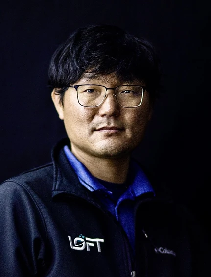
Associate Professor, Wyant College of Optical Sciences, Arizona state university, USAOptical Trilogy: Design, Fabrication, and Testing for Astronomical Telescopes

Upendra N. Singh
NASA Technical Fellow for Sensors and Instrumentation, NASA Engineering and Safety Center (NESC), NASA Langley Research Center, USANASA Sensors and Instrumentation: Driving Technologies to Enable an Innovative and Prosperous Future
Dr. Upendra N. Singh, NASA Technical Fellow for Sensors and Instrumentation at NASA Engineering and Safety Center (NESC), leads a group of multi-disciplinary Sensors and instrumentation expert team from NASA, industry, academia, and Federally Funded Research and Development Center (FFRDC) and conducts independent investigation of NASA tactical challenges; Sensors and Instrumentation assessment; develops approaches to identify, solve and prevent sensors and instrumentation related problems throughout the Agency, as well as developing strategies, plans, and priorities for maintaining and advancing the Sensors and Instrumentation discipline for NASA's critical missions. Dr. Singh has organized over 50 international symposia/conferences and has authored/co-authored over 500 scientific articles in atmospheric sciences and remote sensing area. He is an elected fellow of the International Society of Optical Engineering (SPIE), the Optical Society of America (OSA), the Indian Meteorological Society and a Senior Member of IEEE. He served on the Board of Director for the Society of Photo-Optical Instrumentation Engineers (SPIE) during 2009-11, and the President of International Coordination Group of Laser Atmospheric Studies (ICLAS) of International Radiation Commission (IRC) during 2008-2015.
Dr. Singh has received numerous awards and honors, including the NASA Outstanding Leadership Medal (2016, 2001); NASA Langley's H.J.E. Reid Award (2005) and NASA's Exceptional Service Medal (2006).
S6. Biophotonics and Biomedical Imaging
楊東霖 T. Tony Yang
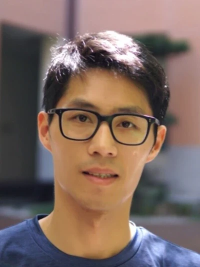
Associate Professor, Department of Electrical Engineering, National Taiwan UniversityExpansion localization microscopy unravels the molecular-resolution constitution of mammalian centrioles

George Barbastathis
Professor, Department of Mechanical Engineering, Massachusetts Institute of Technology, USAOptical real-time monitoring of complex processes
George Barbastathis received the Diploma in Electrical and Computer Engineering in 1993 from the National Technical University of Athens (Εθνικό Μετσόβιο Πολυτεχνείο) and the MSc and PhD degrees in Electrical Engineering in 1994 and 1997, respectively, from the California Institute of Technology (Caltech.) After post-doctoral work at the University of Illinois at Urbana-Champaign, he joined the faculty at MIT in 1999, where he is now Professor of Mechanical Engineering and holds the Singapore Research endowed chair. He has worked or held visiting appointments at Harvard University, the Singapore-MIT Alliance for Research and Technology (SMART) Centre, the National University of Singapore, and the University of Michigan - Shanghai Jiao Tong University Joint Institute (密西根交大學院) in Shanghai, People's Republic of China. His research interests are in machine learning and optimization for computational imaging and inverse problems; and optical system design, including artificial optical materials and interfaces. He is member of the Society for Photo Instrumentation Engineering (SPIE), the Institute of Electrical and Electronics Engineering (IEEE), and the American Society of Mechanical Engineers (ASME). He is a Fellow of the Optical Society of America (OSA) and the Society for Photo Instrumentation Engineering (SPIE) and between 2019-2024 served as Associate Editor for the journal Optica.
根本知己 Tomomi Nemoto
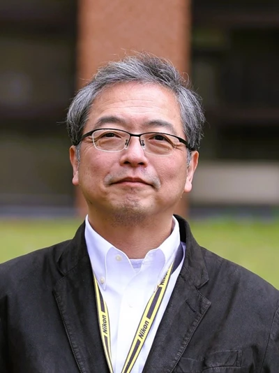
Professor, Biophotonics Research Group, Exploratory Research Center on Life and Living Systems (ExCELLS), National Institute of Natural Sciences, JapanAdvancements in in vivo Two-Photon Microscopic Imaging in the Mouse Brain through Novel Optical Technologies
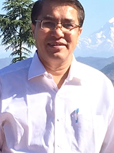
Dalip Singh Mehta
Professor, Department of Physics, Indian Institute of Technology DelhiOptical Coherence Microscopy and Nanoscopy using Spatial Coherence Engineering: Speckle-free Quantitative Phase Imaging of Biological Cells with High Spatial and Temporal Phase Sensitivity and High Space Bandwidth Product
Dr. Dalip Singh Mehta is currently a Professor at the Department of Physics since 2012, Indian Institute of Technology Delhi. Previously, he worked as Associate Professor and Assistant Professor (June 2002 - Dec. 2012), Indian Institute of Technology Delhi. Before Joining the Institute, he was JSPS Post-Doctoral Fellow (July 2000 - June 2002) at the University of Electro-communications, Tokyo, Japan, Post-Doctoral Fellow National Dong Hwa University, Taiwan (Nov. 1999–May 2000) Research Associate, NPL, New Delhi, STA Post-Doctoral Fellow (June 1997 – May 1998), NIRE, Tsukuba, Japan and UNESCO Research Fellow (Jan. 1996 – Sept.1996), Tokyo Institute of Technology Tokyo, Japan.
He has contributed more than 205 research papers in International Refereed Journals, and more than 240 in International and National Conferences. He has delivered more than 95 Invited Talks/Lectures in various International and National Conferences and Universities. He has supervised 28 Ph. D. students and currently supervising 11 Ph. D. students. He has also supervised more than 95 M. Tech./B. Tech. /M.Sc. students’ major projects. He has filed 15 patents out of which 12 patents awarded and 3 Technologies Transferred to Industry.
Research Interests:
Bio-photonics & Biomedical Optical Imaging: Optical Coherence Tomography, Label-free Quantitative Phase Microscopy & Nanoscopy, Multi-modal Optical Imaging and Spectroscopic Point-of-care Devices for Oral and Cervical Cancer fast screening, Diagnosis & Detection.
Quantitative phase microscopy (QPM) has recently become indispensable technology for label-free quantitative analysis of various biological cells and tissues for early-stage disease detection. Using QPM one can determine the variation of refractive index and thickness precisely, cell dry mass concentration, cell membrane fluctuation, sickle cell imaging, hemoglobin concentration, etc. The key parameters controlling measurement accuracy and capability of any QPM systems depend on its spatial and temporal phase sensitivity, speckle-free imaging and high space-bandwidth product. Most QPM techniques utilize highly coherent light sources like lasers benefited by their remarkable properties, such as, high spatial and temporal coherence, and brightness. High spatio-temporal coherence leads to occurrence of speckle noise and spurious fringes leading to inhomogeneous illumination and poor spatial phase sensitivity. We report coherent-noise free QPM with an order of magnitude improved spatial phase sensitivity, space-bandwidth product and high temporal phase. The results of QPM images of biological cells are compared with low temporal coherence and high coherence light. We found that using spatially partially coherent light a speckle-free and unform illumination over large field-of-view. The uniform illumination leads to large interferometric field-of-view leading to the reconstruction of phase map of large no of biological cells in single shot manner [1-8].
Experimental results of complete reconstruction of sperm cells with high accuracy are demonstrated. We could differentiate between the healthy and unhealthy sperm cells and oxidative stressed and unstressed conditions. Further, using quantitative phase we could perform nanoscopy using multiple signal classification algorithm (MUSICAL). These findings can be used for IVF technology. The QPM was further used for cell-to-cell interaction using common path interferometer with speckle-free and high temporal stability [5-8]. More recently we have developed speckle-free hyperspectral quantitative phase microscopy for biological cells and tissues [9-10]. The technique was applied for phase imaging of cancer cells. Using hyperspectral QPM decoupling of refractive index and thickness of transparent cells and samples. Finally, the QPM system was combined with optical tweezers system and phase map of waveguide trapped polystyrene spheres and biological cells is reconstructed.
Keywords: Phase Microscopy, Spatial Coherence, Phase Sensitivity, Bandwidth Product.
- References:
- Quantitative Phase Microscopy and Tomography: Techniques using partially spatially coherent monochromatic light, Dalip Singh Mehta, Ankit Butola, Veena Singh, IOP Publishing 2022.
- Virendra Kumar, Atul Kumar Dubey, Mayank Gupta, Veena Singh, Ankit Butola, Dalip Singh Mehta, Speckle noise reduction strategies in laser-based projection imaging, fluorescence microscopy, and digital holography with uniform illumination, improved image sharpness, and resolution, Optics & Laser Technology 141, 107079 (2021).
- A. Ahmad, Vishesh Dubey, Nikhil Jayakumar, Anowarul Habib, Ankit Butola, Mona Nystad, Ganesh Acharya, Purusotam Basnet, Dalip Singh Mehta, Balpreet Singh Ahluwalia, “High-throughput spatial sensitive quantitative phase microscopy using low spatial and high temporal coherent illumination,” Scientific Reports 11, 1 (2021).
- A. Butola, D. Popova, D. K. Prasad, A. Ahmad, A. Habib, J. C. Tinguely, P. Basnet, P. Senthilkumaran, D. S. Mehta and B. S. Ahluwalia, “High spatially sensitive quantitative phase imaging assisted with deep neural network for classification of human spermatozoa under stressed condition” Scientific Reports 10, 1(2020).
- A. Butola, Sheetal Raosaheb Kanade, Sunil Bhatt, Vishesh Kumar Dubey, Anand Kumar, Azeem Ahmad, Dilip K Prasad, Paramasivam Senthilkumaran, Balpreet Singh Ahluwalia, Dalip Singh Mehta, “High space-bandwidth in quantitative phase imaging using partially spatially coherent digital holographic microscopy and a deep neural network, Optics Express 28, 36229 (2020).
- R. Singh, V. Dubey, D. Wolfson, A. Ahmad, A. Butola, G. Acharya, D. S. Mehta, P. Basnet, B. S. Ahluwalia , “Quantitative assessment of morphology and sub-cellular changes in macrophages and trophoblasts during inflammation” Biomedical Optics Express 11, 3733 (2020).
- Ankit Butola, David A Coucheron, Karolina Szafranska, Azeem Ahmad, Hong Mao, Jean-Claude Tinguely, Peter McCourt, Paramasivam Senthilkumaran, Dalip Singh Mehta, Krishna Agarwal, Balpreet Singh Ahluwalia, Multimodal on-chip nanoscopy and quantitative phase imaging reveals the nanoscale morphology of liver sinusoidal endothelial cells, PNAS-Proceedings of the National Academy of Sciences 118 (47) (2021), pp. e2115323118.
- Dalip Singh Mehta, Shilpa Tayal, Azeem Ahmad, Sunil Bhatt, Vishesh Kumar Dubey, Ankit Butola, Balpreet Singh Ahluwalia, Effect of partial spatial coherence of light on quantitative phase microscopy of biological samples: improved spatial phase sensitivity, space-bandwidth product, and high accuracy in phase measurement, Proceedings of SPIE BiOS Vol. 12389, Quantitative Phase Imaging IX; 123890L (2023).
- Anuj Saxena, Azeem Ahmad, Vishesh Dubey, Anowarul Habib, Satish Kumar Dubey, Balpreet Singh Ahluwalia & Dalip Singh Mehta, Dynamic quantitative phase imaging using calcite crystal-based temporally stable interferometer, J. Mod. Opt. 70 (19-21), 973-982 (2024).
- Himanshu Joshi, Bhanu Pratap Singh, Ankit Butola, Varun Surya, Deepika Mishra, Krishna Agarwal and Dalip Singh Mehta, Compact Linnik-type hyperspectral quantitative phase microscope for advanced classification of cellular components Compact Linnik-type hyperspectral quantitative phase microscope for advanced classification of cellular components J. Biophotonics 17(8), 1-11 (2024).
S7. Display and Solid State Lighting
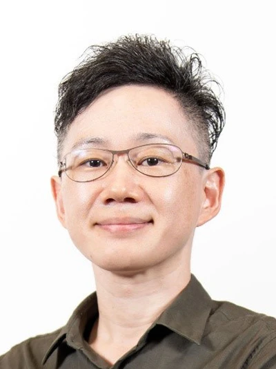
嘉部量太 Ryoto Kabe
Assistant Professor, Okinawa Institute of Science and Technology Graduate University, JapanPersistent and stimulated luminescence of organic semiconductors
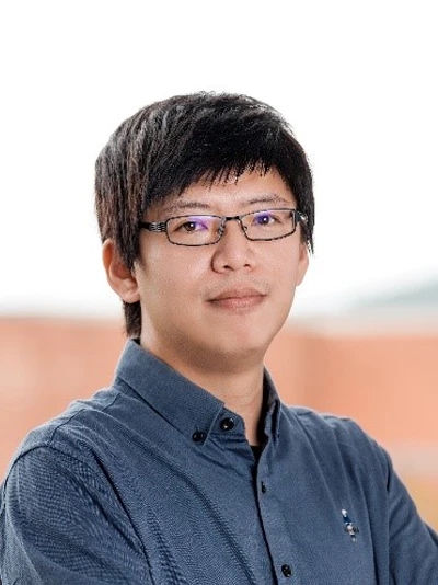
王俊達 Chun-Ta Wang
Associate Professor, Department of Photonics, National Sun Yat-sen UniversitySwitchable Liquid Crystal Polarization Volume Gratings: Design and Applications
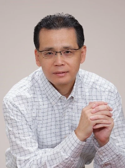
大江昌人 Masahito Oh-e
Professor, Institute of Photonics Technologies, Department of Electrical Engineering, National Tsing Hua UniversityNovel switching of liquid crystals for use in rapid THz modulation: Mastering liquid crystals beyond displays
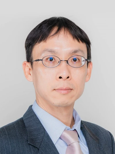
賴昆佑 Kun-Yu Lai
Professor, Department of Optics and Photonics, National Central UniversityDetecting cancer by the plasmonic effect of InGaN quantum wells
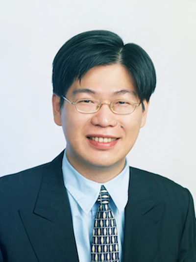
李君浩 Jiun-Haw Lee
Professor, Graduate Institute of Photonics and Optoelectronics, National Taiwan UniversityTriplet management of blue organic light-emitting diode for higher efficiency and longest lifetime
Prof. Jiun-Haw Lee received BS and Ph. D degree in electrical engineering in 1994 and 2000, respectively, from National Taiwan University. From 2000 to 2003, he was with the RiTdisplay Corporation as the director. Since 2003, he joined the faculty of National Taiwan University in the Graduate Institute of Photonics and Optoelectronics and the Department of Electrical Engineering, where he is currently a professor.
His research interests include display technologies, organic light-emitting diode, thin-film solar cells, organic solar cell, optoelectronic devices. Prof. Jiun-Haw Lee has done many pioneering works in the areas of carrier and exciton dynamics of organic thin-film device, as well as photonic design of organic light-emitting diode (OLED). He is fellow of Optica, SID, and SPIE.
S8. Energy Photonics and Sustainable Technology
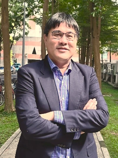
劉振良 Cheng-Liang Liu
Professor, Department of Materials Science and Engineering, National Taiwan UniversityOrganic/Hybrid Thermoelectric Materials and Devices
Prof. Cheng-Liang Liu is a Professor of Materials Science and Engineering at National Taiwan University. He received the B.S. and Ph.D. degrees in Chemical Engineering from National Taiwan University in 2002 and 2007, respectively. He then worked as visiting scientist at the University of Washington (USA) from 2005 to 2006, postdoctoral fellow at National Taiwan University from 2008 to 2010, Assistant Professor at Yamagata University (Japan) from 2010 to 2012, Assistant and Associate Professor at National Central University (Taiwan) from 2012 to 2020, before joining National Taiwan University in 2020. His group focuses on exploring organic polymers and hybrid materials, targeting electronic and energy applications, including transistors, memory devices, solar cells, and thermoelectrics. He currently serves as Associate Editor for Polymer Journal and Journal of Taiwan Institute of Chemical Engineers.
For more information, please visit our website.
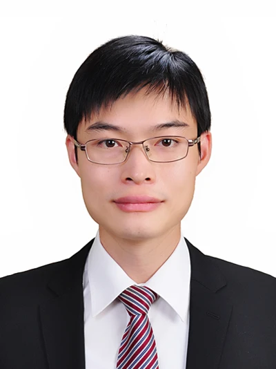
劉昌樺 Chang-Hua Liu
Associate Professor, Institute of Electrical Engineering, National Tsing Hua UniversityAdvancing Sustainable Mid-Infrared Optoelectronics with Black Phosphorus-Based van der Waals Heterostructures
The development of high-performance, sustainable and silicon-compatible mid-infrared optoelectronics is crucial for advancing on-chip sensing and spectroscopic technologies. Traditionally, these devices have relied on III-V/II-VI compound semiconductors, which often face performance limitations due to lattice and thermal mismatches at heterointerfaces. Black phosphorus (BP), with its direct and narrow bandgap (approximately 0.3 eV in bulk), offers a promising alternative. Its van der Waals (vdW) nature allows for seamless integration onto various substrates and photonic structures, making BP-based optoelectronics highly suitable for mid-infrared integrated photonics.
This talk outlines the design of mid-infrared photodetectors using BP-based van der Waals (vdW) heterostructures, which offer linear dichroism, broad spectral sensitivity (from visible to mid-infrared), high external quantum efficiency, and rapid operation (exceeding 200 MHz) at room temperature. These photodetectors can be seamlessly integrated with silicon waveguides. Additionally, we will demonstrate how vdW engineering of BP-based heterostructures enables the realization of mid-infrared emitters with long-term stability and electrically tunable wavelength and polarization features. These advancements hold significant potential for mid-IR sensing, data processing, and imaging technologies.
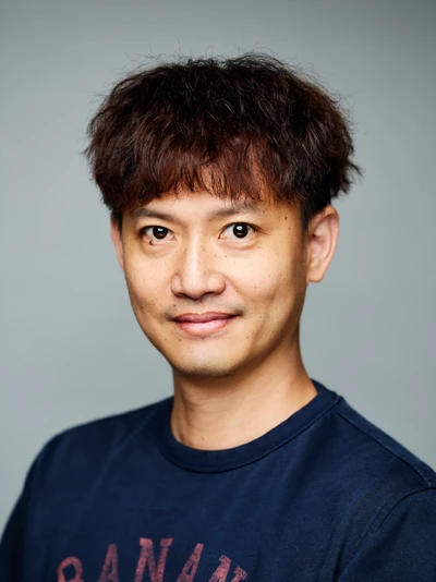
黃裕清 Yu-Ching Huang
Professor, Department of Materials Engineering, Ming Chi University of TechnologyTowards Highly Efficient 4-Terminal Perovskite/Si Tandem Solar Cells
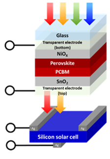
With the increasing global focus on achieving net-zero carbon emissions, improving the efficiency of low-carbon energy has emerged as a key strategy for reducing carbon footprints. Perovskite solar cells (PSCs) have received much attention due to their long exciton diffusion length, high carrier mobility, and tunable bandgap. Although the current power conversion efficiency (PCE) of single-junction PSCs exceeds 26%, which is comparable to that of silicon solar cells, this efficiency is close to the Shockley-Queisser (SQ) limit. To further improve the PCE of single-junction solar cells, tandem solar cells, in which the top cell with high energy bandgap is paired with the bottom silicon solar cell are a promising solution for breaking through the SQ limit. Compared to single-junction solar cells, tandem solar cells effectively reduce thermalization and sub-bandgap absorption losses by rationally distributing the absorption of sunlight between the top and bottom cells. Therefore, well-designed semi-transparent wide-bandgap PSCs are a prerequisite for the realization of high-efficiency tandem solar cells. However, the efficacy of wide bandgap PSCs is hampered by photo-induced phase separation and energy level incompatibility, which results in significant open circuit voltage (Voc) losses when the proportion of Br ions exceeds 20%. This present addresses this challenge by partially replacing Br with Cs and refining the composition of the perovskite precursor through cation incorporation. This strategic approach preserves the wide bandgap and improves the photostability of wide bandgap perovskite films. By carefully optimizing these films, the efficiency of the semi-transparent concentrator solar cell was increased to 19.21%, and the PCE of the four-terminal PSC/silicon tandem solar cell reached ~30%.
Keywords: perovskite solar cells, tandem, wide bandgap, phase segregation
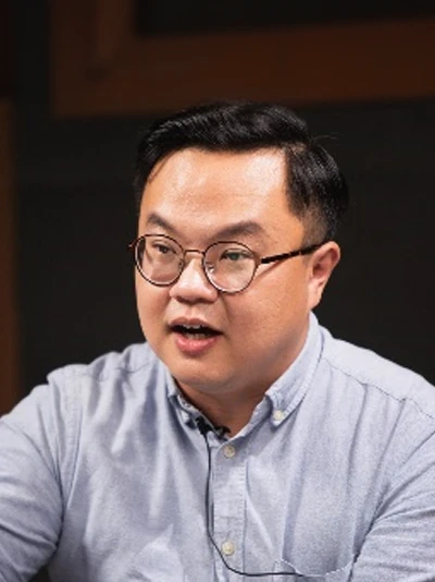
闕居振 Chu-Chen Chueh
Professor, Chemical Engineering, National Taiwan UniversityInterface Design for Efficient Organic, Perovskite and Perovskite/Organic Tandem Solar Cells

洪緯璿 Wei-Hsuan Hung
Professor, Graduate College of Sustainability and Green Energy / Institute of Materials Science and Engineering (IMSE), National Central University (NCU)Title
S9. Optical Sensing
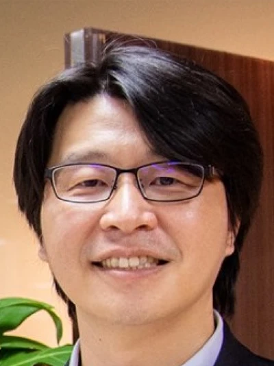
彭朋群 Peng-Chun Peng
Professor, Department of Electro-Optical Engineering, National Taipei University of TechnologyLarge-Scale and High-Capacity Sensing Systems Utilizing Free-Space Optics
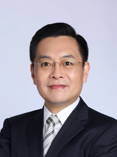
楊富量 Fu-Liang Yang
Distinguishe Research Fellow, Research Center for Applied Sciences, Academia SinicaOutlook for pulse oximeter applications
During the Covid-19 pandemic, the market for pulse oximeters rapidly expanded, as blood oxygen saturation (SpO2) became an important indicator for assessing the severity of a patient's condition. The technology for blood oxygen monitors has reached a mature stage due to their simplicity of use. With numerous manufacturers offering blood oxygen monitor products on the saturated market, competition has grown fierce. To enhance product value and remain competitive, manufacturers must add more features to their products, such as new indicators or abnormality detection functions. Incorporating blood pressure and blood glucose measurements, as well as atrial fibrillation (AFib) detection, into pulse oximeter is on our priority list, due to they are indications for ischemic heart diseases, stroke, and diabetes. When arrhythmias occur, patients need to be vigilant, especially since atrial fibrillation increases the risk of stroke fivefold, making early warning crucial. While the gold standard for AFib detection is through analyzing 12-lead electrocardiogram (ECG) signals, the photoplethysmogram (PPG) signal measured by oximeters also originates from the cardiac cycle, allowing it to extract heart rate variability features with additional information on blood flow volume. Out of the 460 testing data points, the method had only 2 false-positive results and 0 false-negative results. Our innovative AI-based, non-invasive blood glucose meter requires only one calibration is needed for users not affected by medications. For complicated medication subjects, our best practice (Deduction Learning) shows only 12 calibration data points are required to achieve 90% accuracy. In addition, the original AI Deduction Learning method was also utilized and modified to accurately measure blood pressure, with the aforementioned pulse oximeter. This extended functionality offers a more comprehensive physiological health monitoring, allowing users to obtain more physiological indicators through a single simple pulse oximeter. Providing early warning and preventive measures, it helps users better manage and prevent cardiovascular and cerebrovascular diseases.
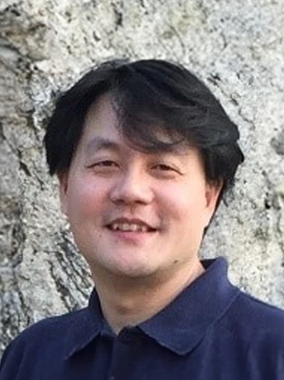
ChengKuo, Vincent, Lee
Professor, National University of SingaporeCMOS Photonics Platform – Sensing and Computation

Wanvisa Talataisong
Research Fellow, School of Physics, Suranaree University of Technology, ThailandOptical fiber sensing device: Future technology for environmental monitoring
Over the past century, the world's population has surged, resulting in a rapid expansion of industrial manufacturing plants. Thailand, particularly its capital Bangkok, has experienced significantly worsening air quality since early 2019. Pollution levels, including PM2.5 and greenhouse gases including carbon dioxide (CO2), methane (CH4), and nitrogen dioxide (NO2) remain hazardous in many parts of Bangkok and its surrounding provinces.
Methane (CH4) is a potent greenhouse gas with a 100-year global warming potential which is ~80 times higher thermal absorption and radiation than that of carbon dioxide. Its atmospheric mixing ratio has increased more than two-fold since the preindustrial period, contributing ~20% of the radiative climate forcing for all greenhouse gases. Future anthropogenic impacts on the atmospheric CH4 budget are not restricted to direct emissions but also include climate-driven perturbation of the natural CH4. This motivates recent efforts to place strong baseline constraints on natural CH4 sources and understand their environmental sensitivity. Oceanic emissions represent a highly uncertain term in the natural atmospheric methane (CH4) budget, due to the sparse sampling of dissolved CH4 in the marine environment.
Research in the developing of Greenhouse gas monitoring and mitigation strategies is of great interest. Numerous Greenhouse gas sensing methods have been developed over the past decade. Among these, optical-based monitoring techniques have proven ideal for remote and real-time detection of particles and gases. Therefore, this research proposes an environmental monitoring system comprising two optical systems:
- Optical fiber SPR sensor using the Kretschmann configuration working together with a gold nano-thin film for CH4 and CO2 detection. The concentration of Greenhouse gas in liquid can be detected by depositing a selective material on metal surface (gold nano-thin film) of SPR system that can change its refractive index with the variation of the concentration of CO2 or CH4. Then, the concentration of CO2 or CH4 can be analyzed from the optical fiber SPR sensor.
- Hollow-core polymer optical fiber specific absorption characteristics of CO2 and CH4 occurring in the mid-IR region spanning from 2 to 12 microns. The concentration of gas can be deduced from absorption measurements by knowing the absorption strength of CO2 and CH4 at specific optical frequencies. This approach eliminates functionalization procedure and necessity of regular recalibration.
Optical Society of Japan
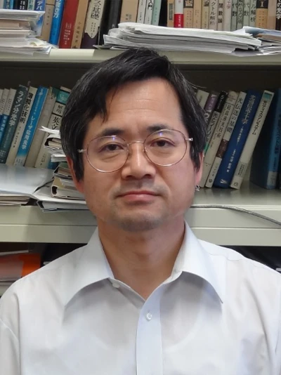
佐藤学 Manabu Sato
Professor, Graduate School of Science and Engineering, Yamagata University, JapanSuper-frequency resolution using sub-bin in discrete Fourier transform and application
Manabu Sato is a Professor in Yamagata University and a Visiting Researcher in RIKEN Center for Advanced Photonics.
He received B.S. from Yamagata University, M.S. in graduated school of electronics engineering from Tohoku University in 1986, worked at Hitachi Research Laboratory in Hitachi Ltd. until 1989, and joined Ishinomaki Senshu University. He returned to Research Institute of Electrical Communications in Tohoku University in 1993, and studied on the nonlinear optics using nonlinear crystals such a periodically poled LiNbO3 (PPLN) crystal to generate mid infrared waves to THz waves. He received his Ph.D. from Tohoku University in 1994. He also joined Optoelectronics Research Center in University of Southampton in UK as a Visiting Researcher from 1996 to 1997 to study on the contact method to fabricate PPLN. He moved to Yamagata University in 1998, and started studying on the optical sectional imaging such as optical coherence tomography (OCT). He studied on a synthesized light source, single shot full field OCT, and low invasive 2D probe, and applied the multi-mode fiber for the optical communications to imaging 3D OCT images of in vivo rat brain. He also joined the Tera-Photonics Research Team in RIKEN in 2019. Recently, his research fields gradually spread to signal processing to extract new information. He is a member of Optica, the Japan Society of Applied Physics, and is a director of the optical society of Japan.
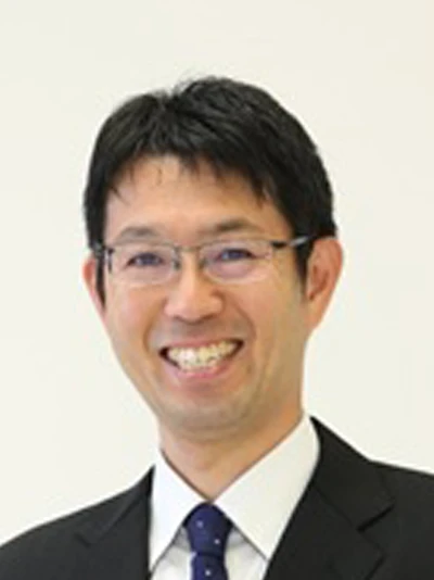
渡邉歴 Wataru Watanabe
Professor, Department of Electrical & Electronic Engineering, College of Science and Engineering, Ritsumeikan University, JapanExtraction of spectral features from speckle in imaging through diffusers
Wataru Watanabe is a professor at Ritsumeikan University. He received his BS, MS, and Doctor of Engineering degrees from Osaka University in 1994, 1996, and 1999, respectively. During 1999-2006, he was an assistant professor at the Graduate School of Engineering, Osaka University. During 2006 to 2013, he was a researcher at the National Institute of Advanced Industrial Science and Technology (AIST). He joined Ritsumeikan University in 2013 as a professor.
His current research interests include ultrafast laser micromachining and biomedical optics.
Optical Society of Korea
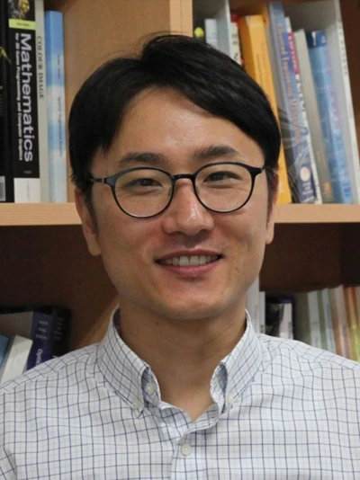
Jae-Hyeung Park
Associate Professor, Department of Electrical and Computer Engineering, Seoul National University, South KoreaFocus cue and occlusion supporting AR near eye displays
